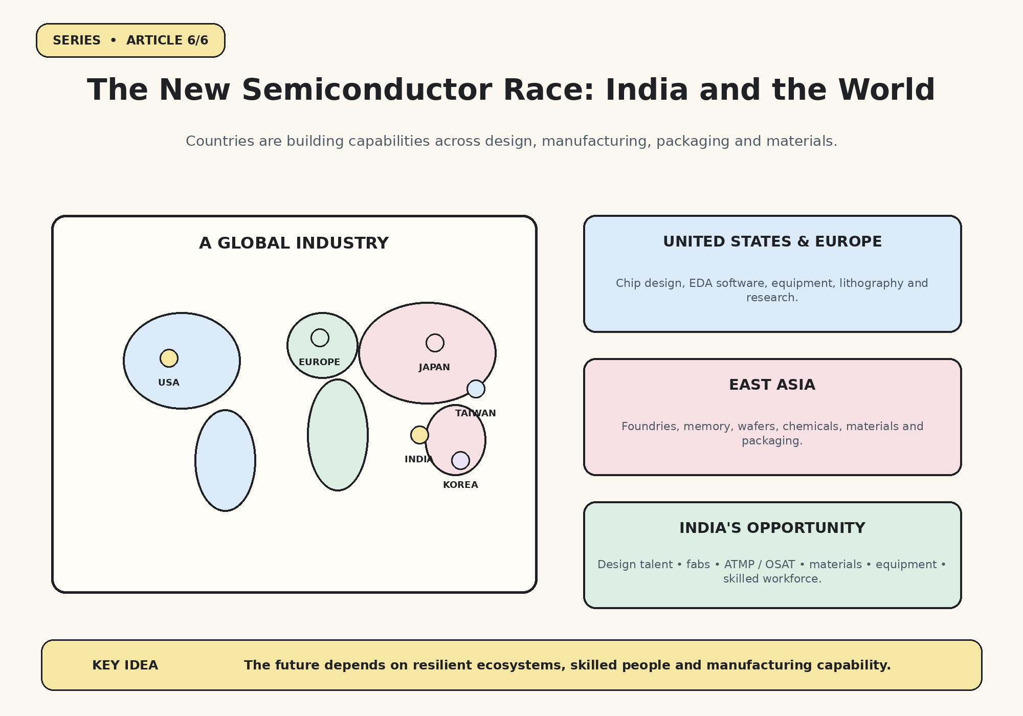
Why governments are investing billions, why chip factories matter to national strategy, and how India is trying to build a place in one of the world’s most demanding industries.
A semiconductor chip may be smaller than a coin. But the ability to design and manufacture it influences artificial intelligence, telecommunications, cars, defence systems, healthcare, energy and almost every modern industry.
That is why semiconductors are no longer treated as just another electronics component.
They are strategic infrastructure.
Countries want reliable access to chips, companies want secure manufacturing capacity, and governments are investing in the factories, talent and suppliers needed to support the next generation of computing.
1. Why has the semiconductor race become so important?
Three forces are driving the race.
AI and data centres. Training and running advanced AI systems requires enormous computing capacity, memory bandwidth and energy. Demand for GPUs, custom accelerators, networking chips and HBM has increased the importance of advanced manufacturing and packaging.
National security. Chips are used in communications, aerospace, defence, infrastructure and industrial control systems. Governments want resilient access to critical technologies and do not want essential supply to depend on a single vulnerable location.
Economic value. Semiconductor factories create high-skilled jobs and support wider ecosystems in materials, chemicals, precision equipment, construction, logistics, software and research.
A fab is not just a factory. It is an anchor for a much larger industrial network.
2. The world does not have one semiconductor capital
Different regions have developed different strengths.
| Region | Important strengths | Examples |
|---|---|---|
| United States | Chip design, EDA, processor IP, equipment and systems | NVIDIA, AMD, Qualcomm, Apple, Synopsys, Cadence, Applied Materials, Lam Research, KLA |
| Taiwan | Leading foundry manufacturing and advanced packaging | TSMC, UMC, ASE |
| South Korea | Memory and advanced semiconductor manufacturing | Samsung, SK hynix |
| Japan | Silicon wafers, photoresists, chemicals and manufacturing equipment | Shin-Etsu, SUMCO, JSR, TOK, Tokyo Electron, SCREEN |
| Netherlands | Advanced lithography systems | ASML |
| Germany and wider Europe | Optics, materials, equipment and power semiconductors | ZEISS, Siltronic, Infineon, STMicroelectronics |
| China | Large domestic chip market, manufacturing, materials and equipment development | SMIC and a growing domestic supplier ecosystem |
| India | Chip design talent, emerging fabrication, assembly and testing | Tata Electronics, Micron, Kaynes, CG Semi and design centres |
This is a map of important strengths, not a list of exclusive capabilities. Companies operate across borders, and every region depends on international suppliers.
3. Why countries want fabs of their own
A leading-edge semiconductor fab requires enormous capital, specialist equipment, reliable power and water, highly trained engineers, strict process control and a stable supplier network.
It can take years to build and qualify a new facility. Even after construction, reaching consistent production yield is a difficult engineering challenge.
So why invest?
Because a country with local manufacturing and packaging capacity can:
- Improve resilience for selected chip categories.
- Develop local engineering and manufacturing talent.
- Attract suppliers and downstream electronics companies.
- Build experience in process technology and quality.
- Reduce exposure to some international supply disruptions.
But self-sufficiency is not realistic for every country in every part of the chain. The practical goal is usually to build strategic capabilities while remaining connected to the global ecosystem.
4. India’s semiconductor journey: the ambition
India has long had a strong presence in semiconductor design and engineering services. Many global semiconductor companies have major engineering and R&D teams in India.
The next ambition is to expand from design into a broader ecosystem: wafer fabrication, assembly, testing, packaging, materials, equipment, research and talent development.
The India Semiconductor Mission and Semicon India Programme were created to support this transition.
In July 2026, the Union Cabinet approved Semicon 2.0, with a stated budget outlay of ₹1,27,500 crore. The programme identifies six pillars: design, machines and materials, more fabs, ATMP/OSAT, research and development, and talent development.
The same government update reported 12 approved manufacturing units with cumulative investment commitments above ₹1.64 lakh crore. It said Micron, Kaynes and CG Semi had started commercial production, while the first silicon fab was scheduled for commissioning in 2028. These are government-reported milestones and plans; project status can change as facilities ramp. Government of India, Semicon 2.0 announcement, 15 July 2026.
5. India’s projects: understand what each one is building
The projects are not all the same. Some focus on wafer fabrication. Others focus on packaging, assembly, testing or specialised semiconductor materials.
Wafer fabrication and compound semiconductors
Tata Electronics and PSMC — Dholera, Gujarat
A major silicon wafer fab project developed with Taiwan’s Powerchip Semiconductor Manufacturing Corporation. The announced technology mix includes 28 nm, 40 nm, 55 nm and 110 nm process technologies, aimed at products such as power management, display drivers, microcontrollers and other applications.
These are important production nodes for many industrial, automotive and consumer products. They are not the same as the most advanced leading-edge logic processes used for the newest high-end CPUs and GPUs.
SiCSem — Odisha
A silicon carbide (SiC) semiconductor project. SiC is a wide-bandgap material useful in high-voltage and high-temperature power electronics, including EV power systems, fast chargers, renewable-energy inverters and industrial applications.
Other specialised fabrication
India’s approved ecosystem also includes projects in compound semiconductors and integrated display-related technologies. These serve different markets from conventional silicon logic fabs.
Assembly, testing and packaging
Micron — Sanand, Gujarat
Micron’s facility focuses on assembly and test for memory products. It takes DRAM and NAND wafers produced through Micron’s global manufacturing network and converts them into finished memory and storage products.
This is a critical part of the supply chain, but it is not the same as fabricating the original DRAM or NAND wafers in India.
Kaynes Semicon — Sanand, Gujarat
An OSAT project focused on semiconductor assembly and testing. The government reported commercial production beginning in 2026.
CG Semi with Renesas and Stars Microelectronics — Sanand, Gujarat
An assembly and test project that combines Indian manufacturing investment with international semiconductor partners. The government reported commencement of commercial production in July 2026.
Tata Semiconductor Assembly and Test — Morigaon, Assam
A large assembly and test project intended to expand India’s backend manufacturing footprint.
HCL and Foxconn — Uttar Pradesh
A project focused on display driver integrated circuits and related semiconductor manufacturing capabilities.
Other approved projects
The wider programme includes advanced packaging, silicon carbide, discrete devices and other specialised semiconductor facilities involving companies such as 3D Glass Solutions, CDIL and ASIP.
For the latest project-by-project status, use official government releases and company announcements. Approval, groundbreaking, construction, pilot production and commercial production must not be treated as the same milestone. Government project update, 15 July 2026.
6. Why India’s opportunity is bigger than one fab
A semiconductor ecosystem is not created by building a single factory.
A successful fab needs:
- Reliable, high-quality power.
- Large volumes of ultra-pure water.
- Industrial gases and specialty chemicals.
- Wafer and substrate supply.
- Precision equipment and maintenance.
- Cleanroom construction and environmental controls.
- Process engineers, technicians and quality specialists.
- Customers willing to qualify and buy the output.
India can build capability in several layers at once.
Design and IP: architecture, RTL, verification, physical design, embedded systems and reusable semiconductor IP. India already has homegrown design-services and IP companies — Tata Elxsi, MosChip, Saankhya Labs and Mindgrove among them — alongside the large engineering centres of global chip companies.
ATMP and OSAT: assembly, testing, marking and packaging. This is a practical entry point for building manufacturing discipline, talent and supplier networks.
Materials and chemicals: gases, photoresists, wet chemicals, specialty materials, substrates and purification.
Equipment and components: precision parts, vacuum systems, robotics, inspection systems and process-tool components.
Research and talent: universities, national labs, industry partnerships, cleanroom training and process development.
The long-term opportunity is to connect these capabilities, not to measure success only by the number of announced fabs.
7. Terafab: a different approach to chip supply
In August 2026, SpaceX announced that its Terafab semiconductor project would be built in Grimes County, Texas. The plan is described as a vertically integrated facility combining advanced logic, memory manufacturing, packaging and testing.
The stated motivation is to secure future computing capacity for SpaceX and Tesla systems, including robotics, autonomous vehicles and space-based data-centre ambitions.
The Texas Governor’s office announced a first-phase investment of more than US$16.8 billion and a planned facility of more than 100 million square feet. These are announced project plans, not evidence that the fab is already producing commercial chips. Texas Governor’s announcement, 6 August 2026. SpaceX project update.
Terafab is interesting because it aims to bring logic, memory and advanced packaging under one coordinated manufacturing strategy. But building a fab is only the beginning. The real test will be process qualification, yield, equipment readiness, supplier capacity, talent and the ability to produce reliable chips at scale.
8. What will the next decade of semiconductors look like?
The future is not simply about making transistors smaller.
Several trends are changing how chips are designed and manufactured:
Chiplets and advanced packaging. Instead of building every function on one large die, designers combine specialised dies in a package.
High-bandwidth memory. AI accelerators need to move huge volumes of data quickly, making HBM and memory integration increasingly important.
Specialised processors. CPUs, GPUs, NPUs, networking processors and custom accelerators will coexist, each optimised for different workloads.
Power efficiency. Data centres, vehicles and edge devices need more computation without proportionally increasing energy consumption.
Mature-node manufacturing. Not every chip needs the smallest process node. Power management, microcontrollers, display drivers, sensors and industrial chips continue to use a wide range of established process technologies.
Supply-chain resilience. Governments and companies will continue to diversify manufacturing, materials and packaging capacity.
The takeaway
The semiconductor race is not won by one company, one country or one breakthrough machine.
It is won by building a complete ecosystem: design, IP, software, materials, equipment, fabrication, packaging, testing, talent and customers.
India’s opportunity is real, but it will be measured over years by execution, manufacturing yield, reliable supply, technology depth and global customer trust — not just investment announcements.
The future belongs to the countries and companies that can turn engineering knowledge into reliable manufacturing at scale.
The complete journey
We began with a simple question: who makes a chip?
Across six chapters, we followed the journey:
- The ecosystem: the companies and roles behind a chip.
- The raw materials: silicon, metals, gases, chemicals and water.
- The design and fab: how a blueprint becomes billions of transistors.
- The global supply chain: how countries and specialists work together.
- Packaging and testing: how dies become reliable, usable processors.
- The future: India’s opportunity and the global race to build the next generation of chips.
A tiny chip is the result of an extraordinary amount of human coordination, scientific knowledge and industrial precision.
That is the semiconductor industry: a world of engineering, compressed into a piece of silicon.
Further reading and primary sources
- Government of India — Semicon 2.0 and programme progress, 15 July 2026
- Government of India — Semicon India programme, 1 April 2026
- India Semiconductor Mission — Project overview
- SpaceX — Terafab announcement, 6 August 2026
- Texas Governor — Terafab project announcement
- Semiconductor Industry Association