How a digital blueprint becomes billions of physical transistors — one carefully controlled layer at a time.
A chip designer can spend years building and verifying a processor before a factory makes even one physical copy.
Then comes the FAB — short for fabrication facility.
This is where the design becomes physical: transistors, insulation, contacts and microscopic wiring are constructed on a silicon wafer.
The process is not like printing a photograph once. It is a repeated sequence of highly precise manufacturing operations.
1. First, the factory needs a manufacturing blueprint
Before fabrication, the design team must hand over a final, verified physical layout.
The foundry provides process information, design rules and a Process Design Kit (PDK). The chip designer uses these rules to ensure the layout is compatible with the foundry’s technology.
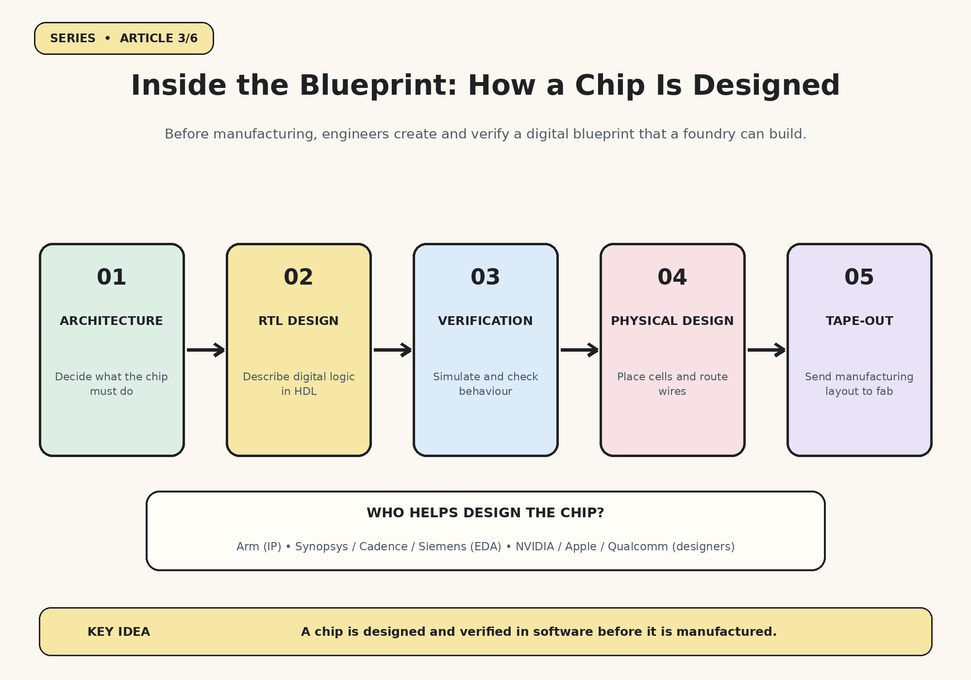
The journey there runs from idea to architecture, logic and layout, then through verification — testing the design in software with enormous simulations — before anything reaches a factory.
The final design data is prepared and released in a milestone called tape-out.
Tape-out does not mean the chip is already made. It means the design is ready to enter the manufacturing flow.
2. Start with a polished silicon wafer
The wafer is a thin, circular slice of single-crystal silicon.
It is cleaned and prepared before layers are formed on its surface. A single wafer can contain many repeated copies of the same chip design, called dies.
The fab must keep the wafer extremely clean. Tiny particles, chemical contamination or process variation can create defects.
3. Build thin films: deposition
The chip is made from multiple materials, not bare silicon alone.
Deposition processes add very thin layers onto the wafer. Depending on the process, these can be insulating, conductive or semiconductor films.
Common families include:
- Chemical Vapour Deposition (CVD).
- Physical Vapour Deposition (PVD).
- Atomic Layer Deposition (ALD).
- Epitaxial growth.
Equipment companies such as Applied Materials, Lam Research, Tokyo Electron and ASM International supply tools used in different deposition and materials processes.
4. Draw a pattern with lithography
This is one of the most remarkable steps.
The wafer is coated with a light-sensitive material called photoresist. A lithography system transfers a carefully designed pattern onto that coating. The pattern itself lives on a photomask — a glass plate carrying the circuit design — which the system projects onto the wafer.
The pattern is developed, leaving selected regions exposed or protected.
ASML is the only commercial supplier of EUV lithography systems. Nikon and Canon also make lithography equipment for other process segments. The lithography ecosystem includes optics, lasers, precision stages and many specialised suppliers — ASML’s EUV machines, for example, depend on ultra-precise mirrors and optics from Germany’s ZEISS.
EUV uses light with a wavelength of approximately 13.5 nanometres.
But lithography is only one step. The pattern must still be transferred into the underlying material.
5. Etch: remove selected material
Etching removes material from regions that are not protected by the pattern.
Depending on the process, etching can be wet-chemical or plasma-based.
The result is a physical structure on the wafer. Repeating lithography and etch steps allows engineers to create increasingly complex patterns.
Lam Research, Tokyo Electron and Applied Materials are among the major suppliers of etch-related equipment.
6. Doping: control electrical behaviour
Silicon’s electrical properties can be modified by introducing carefully controlled impurities.
This process is called doping. Ion implantation is one common method: ions of dopant elements such as boron or phosphorus are accelerated and introduced into selected regions of the wafer, followed by thermal processing where required.
Doping creates regions with different electrical characteristics, which are essential for building semiconductor devices such as transistors.
7. Polish, inspect and measure
As layers accumulate, the surface must be made sufficiently flat for the next steps.
Chemical Mechanical Planarization (CMP) combines chemical action and mechanical polishing to smooth the wafer.
Inspection and metrology tools check dimensions, film thickness, alignment and defects. KLA is a major supplier in process control and inspection.
The fab measures constantly because a process that looks correct in a design file can still vary in physical manufacturing.
8. Repeat — many times
The simplified cycle is:
Deposit → coat → expose → develop → etch → modify → clean → measure → repeat.
A modern chip is built from 50 to 100 or more thin layers, and the full flow can require hundreds or even thousands of individual process steps, depending on how steps are counted and the technology used.
Different layers create transistor structures, insulation and interconnect wiring. The exact process flow is proprietary and differs between foundries and technology generations.
9. The wafer is not the finished product
After fabrication, the wafer is electrically tested. It is then cut into individual dies.
Those dies still need packaging, external connections, thermal management and final testing.
That is the subject of the next stage of the journey.
The takeaway
A semiconductor fab does not simply stamp a chip out of silicon.
It constructs a microscopic system layer by layer, using chemistry, optics, plasma, precision mechanics, electrical engineering and continuous measurement.
The processor begins as a design file. Inside the fab, that design becomes a physical landscape of transistors and wires.
Next: Why a fabricated die is not yet a finished chip — and how packaging, HBM and advanced assembly make modern processors possible.