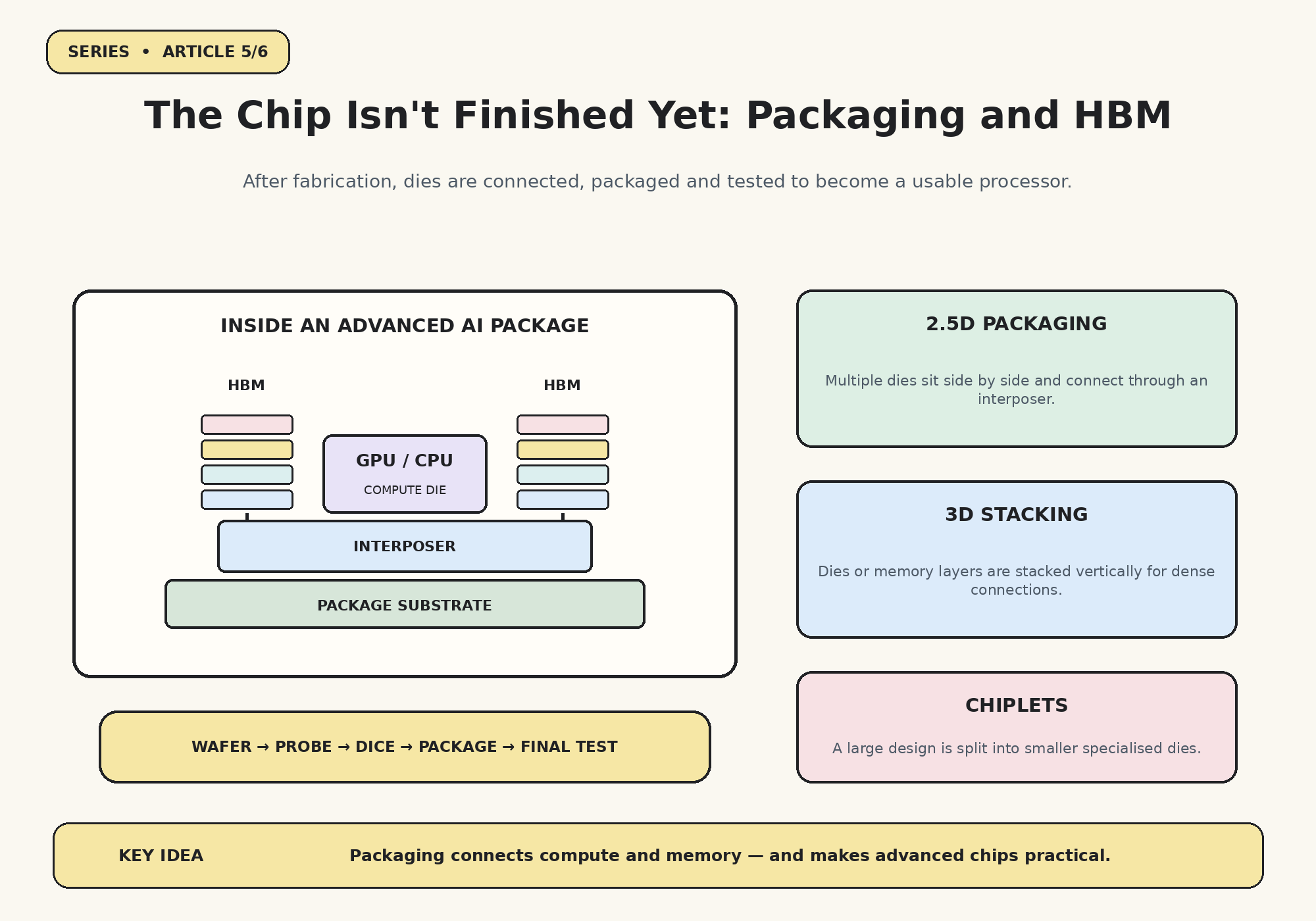
The wafer has been fabricated. The transistors exist. But the chip still isn’t ready for your phone, laptop or AI server.
Imagine a factory has spent months building billions of transistors on a silicon wafer. The wafer finally passes through fabrication.
Is the processor ready?
Not yet.
The wafer is a collection of many individual chip designs, called dies. Those dies must be tested, separated, connected to the outside world, protected, cooled and tested again.
This final stretch is called assembly, packaging and test. And in the age of AI accelerators, it has become one of the most important parts of semiconductor engineering.
1. First, test the wafer
Before cutting the wafer, manufacturers perform electrical tests on individual dies using tiny probes that touch designated contact points.
This stage is commonly called wafer sort or wafer probe.
The test helps identify dies that are defective or do not meet the required electrical specifications. Each die can be mapped by its test result.
Why test before packaging? Because packaging a known-bad die wastes expensive materials, assembly capacity and time.
2. Dice the wafer into individual dies
A wafer may contain hundreds or thousands of repeated die locations, depending on die size and wafer diameter.
A precision dicing process separates the wafer into individual pieces. These pieces are called dies.
A die is the actual piece of semiconductor containing the circuit. It is not yet the complete packaged component that can be mounted on a circuit board.
3. Give the die a package
A package does several jobs at once:
- Protects the fragile silicon from physical damage and contamination.
- Provides electrical connections between the die and the outside system.
- Distributes power and signals.
- Helps move heat away from the silicon.
- Makes the component practical to handle, test and mount.
A simple package may contain one die connected to a substrate. More advanced packages can contain several dies, memory stacks, interposers and multiple layers of connections.
The package is not merely a plastic cover. It is part of the electrical and thermal design.
4. How does a die connect to the outside world?
There are several interconnection approaches.
Wire bonding: Very fine wires connect bond pads on a die to package leads or substrate connections. It remains widely used in many products.
Flip-chip: The die is flipped so that small bumps connect it directly to a substrate or interposer. This can provide many short connections.
Through-silicon vias (TSVs): Tiny vertical electrical connections pass through silicon, enabling certain 3D-stacked structures.
Different products use different combinations. The choice depends on performance, cost, power, package size and reliability requirements.
5. Why modern AI chips need advanced packaging
A high-performance AI processor is often not just one large piece of silicon.
It may need:
- A compute die containing the main processing engines.
- High-bandwidth memory (HBM) placed very close to the compute die.
- A silicon or redistribution-layer interposer to connect the components.
- A package substrate that routes signals and power to the board.
- A thermal solution to remove heat.
This is called heterogeneous integration: bringing different kinds of dies or components together in one package.
Instead of forcing every function onto one giant chip, engineers can combine specialised components that are manufactured using different processes.
6. 2.5D, 3D and chiplets — what do these terms mean?
2.5D packaging: Multiple dies sit side by side and communicate through a high-density interposer or similar routing structure. A GPU and HBM stacks can be integrated this way.
3D stacking: Dies or memory layers are stacked vertically, creating very short connections between layers. This can improve density and reduce the distance signals travel, but introduces difficult thermal and manufacturing challenges.
Chiplets: A large design is divided into smaller specialised dies. For example, compute, I/O and cache functions may be placed on separate chiplets and connected inside one package.
Chiplets can improve flexibility, allow different process technologies to be combined and help manufacturers reuse building blocks. But the connections between chiplets, packaging yield, power delivery and thermal behaviour become critical engineering problems.
7. HBM: memory built for moving enormous amounts of data
A processor can calculate only when data reaches it.
For AI training and inference, moving data between memory and compute units can be a major performance constraint. High Bandwidth Memory (HBM) is designed to provide very high data bandwidth in a compact footprint.
HBM is made by stacking DRAM dies vertically and connecting them using dense interconnects, including through-silicon vias. The memory stack is placed close to the processor, often within the same advanced package.
A simplified view:
- The compute die performs calculations.
- HBM stores the data and model parameters needed by the compute.
- Wide, short connections move data between them.
- The package integrates these components as one system.
HBM is not a replacement for all system memory. It is a specialised high-bandwidth memory used in accelerators and other demanding systems.
Companies such as SK hynix, Samsung and Micron are major HBM suppliers. Their memory products must be designed and qualified to work with the processor and package platform.
8. CoWoS: an example of foundry-level advanced packaging
TSMC’s CoWoS stands for Chip-on-Wafer-on-Substrate. It is an advanced packaging technology used to integrate logic dies and HBM in high-performance systems.
In a simplified CoWoS-S arrangement, logic dies and HBM stacks are connected through a large silicon interposer, which is then integrated with a package substrate.
TSMC describes CoWoS as a platform for high-performance computing and supports different variants, including silicon-interposer and redistribution-layer approaches.
It is one example of how foundries have expanded beyond wafer fabrication into advanced system integration.
Other approaches exist. Intel has technologies such as EMIB and Foveros, while OSAT companies develop their own advanced packaging platforms.
9. Who performs assembly and testing?
Some foundries provide advanced packaging themselves. Other companies specialise in outsourced semiconductor assembly and test — OSAT.
Major OSAT companies include:
- ASE Technology Holding — Taiwan.
- Amkor Technology — United States, with a global manufacturing footprint.
- JCET Group — China.
- Powertech Technology (PTI) — Taiwan.
- SPIL — part of ASE’s group.
Their work can include wafer bumping, dicing, die attach, wire bonding, flip-chip assembly, substrate integration, encapsulation, electrical test and reliability services.
The exact division of work depends on the customer, package type and manufacturing partnership. A modern product may move between a foundry, a specialist packaging partner and a final system assembler.
10. Testing: does the packaged chip really work?
Testing does not end at wafer probe.
After packaging, manufacturers perform electrical and functional tests to confirm that the component meets its specifications. Depending on the product, the flow can include:
- Continuity and connectivity checks.
- Functional testing.
- Performance, frequency and power testing.
- Temperature testing.
- Burn-in or stress testing to screen for early failures.
- Reliability qualification, including selected thermal and mechanical tests.
Specialist companies such as Advantest and Teradyne build the automated test equipment these flows run on.
Not every chip goes through the same test sequence. The requirements depend on whether it is intended for a phone, automotive system, data centre, industrial controller or another application.
Automotive and other safety-critical applications can require especially demanding qualification and traceability.
11. Why packaging has become a bottleneck
For years, much of the industry’s attention focused on shrinking transistors. Today, performance increasingly depends on how compute, memory and other dies are connected.
Large AI packages are difficult to manufacture. They require high-density interconnects, large substrates or interposers, precise alignment, thermal management and strong yields across multiple components.
Recent industry reporting has highlighted advanced packaging capacity as a constraint for AI accelerators, with companies investing in additional CoWoS and alternative packaging capacity. Reuters, 6 November 2026.
This is why packaging is no longer an afterthought. It influences chip architecture, memory choices, system performance and product availability.
The takeaway
Fabrication creates the dies. Packaging connects them, protects them and makes them usable. Testing checks whether the final component can perform reliably.
In advanced processors, the package can bring together compute, memory and multiple specialised dies into one tightly integrated system.
The future of computing is not only about making better transistors. It is also about connecting the right pieces together — faster, closer and more efficiently.
Final chapter: If this industry is so specialised and global, why are countries investing billions to build their own semiconductor capabilities? And where does India fit into the race?