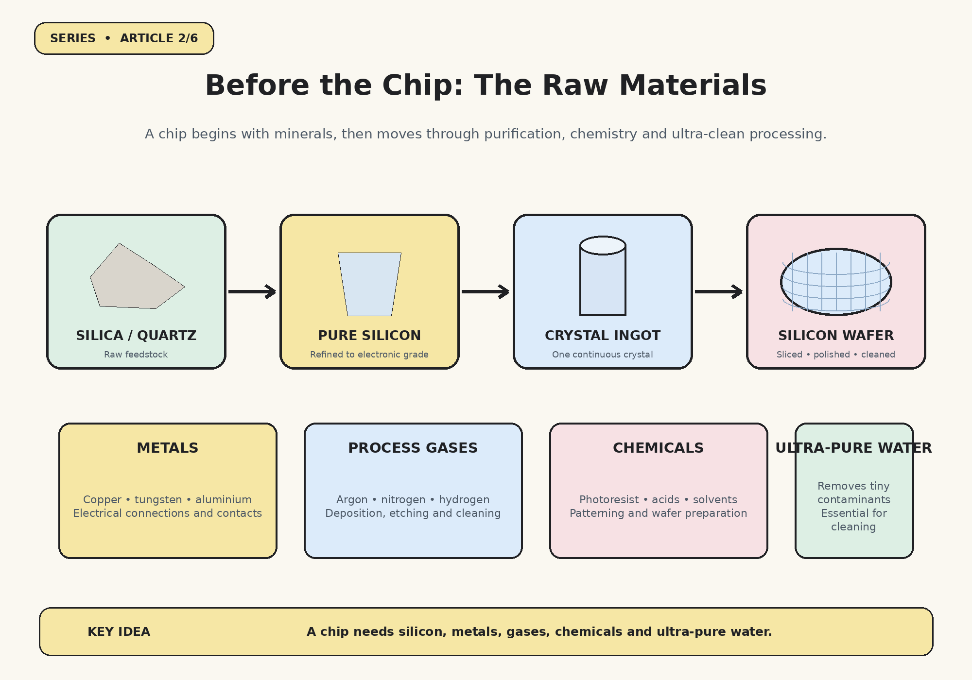
The story of a processor begins long before a cleanroom. It begins with minerals, chemistry, ultra-pure water and suppliers spread around the world.
When you look at a processor, you see a small square of dark material. You don’t see quartz, copper, specialty gases, photoresist, acids, polishing slurry or the thousands of tightly controlled steps that prepared its ingredients.
A semiconductor fab cannot use ordinary industrial-grade materials. It needs materials with purity and consistency measured at extraordinary levels.
Let’s follow the ingredients.
1. Silicon: the foundation, not the whole recipe
Silicon is abundant in Earth’s crust, commonly found in silica-rich materials such as quartz and sand. But ordinary sand cannot be placed directly into a chip factory.
The silicon must be chemically processed and purified into electronic-grade material.
A simplified route is:
Silica-bearing feedstock → metallurgical silicon → chemical purification → electronic-grade polysilicon → single-crystal ingot → wafer.
Electronic-grade polysilicon reaches 99.9999999% purity — “nine nines”, or roughly one impurity atom per billion silicon atoms. It is melted inside a high-purity quartz crucible and grown into a single-crystal ingot, commonly by the Czochralski method. The ingot can be about two metres long. It is then sliced into thin discs around 300 mm — twelve inches — across, ground, polished and cleaned.
Companies active in silicon wafer supply include Japan’s Shin-Etsu Chemical and SUMCO, Taiwan’s GlobalWafers, Germany’s Siltronic and South Korea’s SK Siltron.
These suppliers are not simply selling a disc. They are delivering a highly engineered surface with tightly controlled crystal quality, flatness, thickness and defect levels.
2. Metals: building the chip’s electrical roads
A processor needs a huge network of electrical connections between its transistors.
Different metals and compounds are used for different jobs:
- Copper: widely used for on-chip interconnect wiring.
- Tungsten: used in selected contacts and plugs.
- Aluminium: used in some interconnect and packaging applications.
- Cobalt, ruthenium and other metals: used in selected advanced structures.
- Tantalum- and titanium-based compounds: used in certain barrier, liner and adhesion layers.
- Gold, silver and solder alloys: used in some package connections.
The exact combination changes with the manufacturing process and product. A mining company does not usually ship raw ore to a fab. Material is concentrated, refined, converted into a suitable chemical form and purified before it reaches semiconductor-grade suppliers. Mining and refining specialists such as Freeport-McMoRan (copper), Heraeus (precious metals) and Umicore (specialty metals) operate in these early tiers of the chain.
3. Gases: the invisible ingredients
Inside a fab, gases help create, modify and clean microscopic structures.
Examples include:
- Nitrogen and argon for controlled atmospheres and purging.
- Hydrogen and oxygen for selected process steps.
- Helium for specialised process and cooling applications.
- Neon in certain lithography laser systems.
- Fluorine-containing gases such as carbon tetrafluoride (CF₄) and nitrogen trifluoride (NF₃) for etching and chamber cleaning.
- Silane (SiH₄) and other precursor gases for depositing thin films.
Specialist suppliers include Air Liquide, Linde, Air Products and Taiyo Nippon Sanso, alongside semiconductor-focused gas producers.
A fab needs the right gas, at the right purity, delivered at the right flow and pressure. Contamination can damage a process or reduce yield.
4. Chemicals: painting, dissolving, cleaning and polishing at microscopic scale
A wafer repeatedly goes through coating, exposure, developing, etching, cleaning and polishing.
Some important chemical categories:
| Material | Why it is used |
|---|---|
| Photoresist | Light-sensitive film used to transfer circuit patterns |
| Developer | Reveals the exposed photoresist pattern |
| Hydrofluoric acid | Used in selected oxide etch and cleaning processes |
| Sulfuric acid and hydrogen peroxide | Used in wafer-cleaning mixtures |
| Solvents | Clean or process resist and other materials |
| Deposition precursors | Supply atoms for thin-film layers |
| CMP slurry | Helps chemically and mechanically polish wafer surfaces |
Companies active in semiconductor materials include JSR, Tokyo Ohka Kogyo (TOK), Fujifilm, DuPont, Merck, Entegris, Resonac and Mitsubishi Chemical Group. Each supplies different products and process categories.
5. Water: one of the most overlooked materials
A fab needs large volumes of water, but not ordinary tap water.
Ultra-pure water (UPW) systems remove dissolved ions, organic molecules, particles and microorganisms, purifying water to a resistivity of about 18.2 MΩ·cm — close to the theoretical limit of pure water. Water-treatment specialists such as Kurita, Organo, Evoqua and Veolia participate in this wider industrial ecosystem.
Water is used in wafer cleaning and many process-support operations. It must be treated, monitored and managed continuously.
6. The supply chain is deeper than the supplier’s name
A photoresist supplier may depend on chemical precursors, packaging materials, specialised equipment and energy. A gas supplier may depend on industrial feedstocks, purification systems and cylinder or bulk-delivery infrastructure.
The semiconductor supply chain has multiple tiers. A disruption deep upstream can affect a fab even when the fab’s direct supplier appears healthy.
This is why the industry pays close attention to:
- Geographic concentration.
- Single-source materials.
- Purification capacity.
- Transport and storage.
- Supplier qualification.
- Recycling and strategic inventories.
The Semiconductor Industry Association and McKinsey’s 2026 supply-chain work highlights how dependencies can sit several tiers below a direct supplier. SIA supply-chain report overview.
The takeaway
A chip begins as a network of materials, not as a piece of silicon alone.
The wafer is only the foundation. Metals create connections. Gases and chemicals help build and pattern the structures. Water keeps the process clean. Specialist suppliers make each material reliable enough for semiconductor manufacturing.
Before engineers build a city of transistors, another global industry must first deliver the bricks, tools, chemistry and clean environment.
Next: Once the materials exist, how do engineers design a chip that a factory can actually manufacture?